


![]()
PCB & Enclosure Assembly
![]() SMT Assembly capability: 8 high-speed SMT lines from Yamaha and Sony(10 million chips per day-0402, 0201 with 8 million per day)
SMT Assembly capability: 8 high-speed SMT lines from Yamaha and Sony(10 million chips per day-0402, 0201 with 8 million per day)
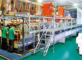
![]() DIP production capability: 3 DIP lines(1.2 million pcs per day)
DIP production capability: 3 DIP lines(1.2 million pcs per day)
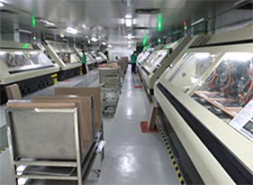
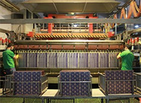
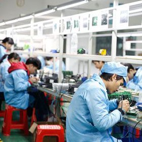
![]() 3 Production Lines for enclosure assembly(Each line has 15 assemblers and 2 quality control engineers)
3 Production Lines for enclosure assembly(Each line has 15 assemblers and 2 quality control engineers)
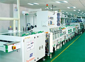
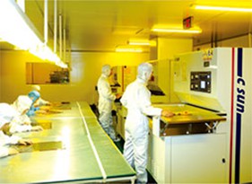
![]() SMT production line: 8 SMT production lines, factory area 6000m2
SMT production line: 8 SMT production lines, factory area 6000m2
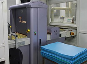
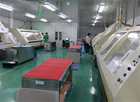
![]() All SMD placements are AOI inspected
All SMD placements are AOI inspected
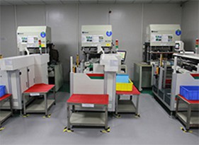
![]() High-end equipment: YAMAHA/JT, AOI/SPI/XRAY, etc
High-end equipment: YAMAHA/JT, AOI/SPI/XRAY, etc
![]() As small as 0.4mm pitch, all BGA placements are X-ray inspected
As small as 0.4mm pitch, all BGA placements are X-ray inspected
![]() Full BOM material supply: RC / bead / inductor / connector / crystal / diode /transistor, etc in stock
Full BOM material supply: RC / bead / inductor / connector / crystal / diode /transistor, etc in stock
![]() Minimum package: 03015, 0201, 0402
Minimum package: 03015, 0201, 0402
![]() One-stop hardware innovation platform: PCB design, board manufacturing, patch assembly, component supply.
One-stop hardware innovation platform: PCB design, board manufacturing, patch assembly, component supply.
![]()
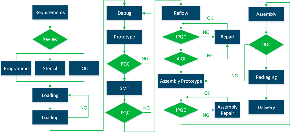
PCB Assembly Workflow
![]()
PCB Assembly Equipment
Main Production and Inspection equipment (8 SMT LINE 3DIP LINE)
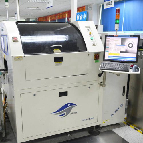
Full-automatic Screen Printer DSP1008
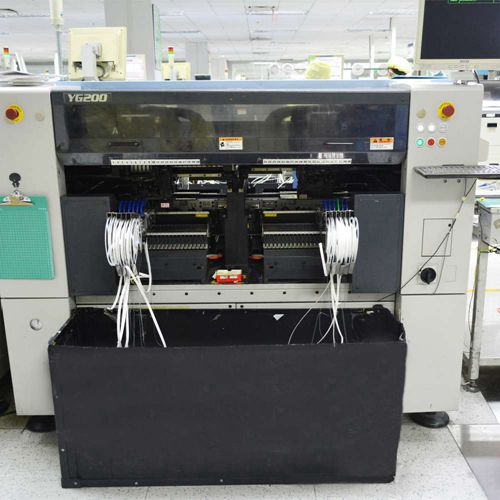
Yamaha YG200 SMT Equipment
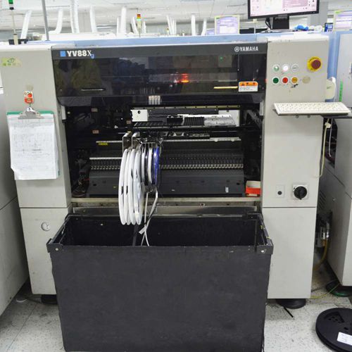
Yamaha YV88-XG SMT Equipment
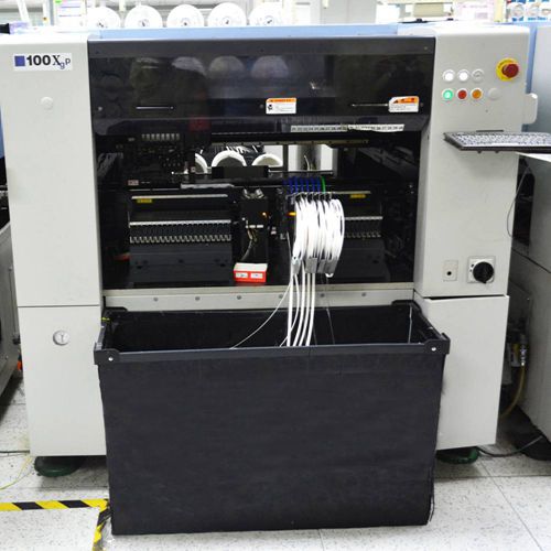
Yamaha YV100XGP SMT Equipment
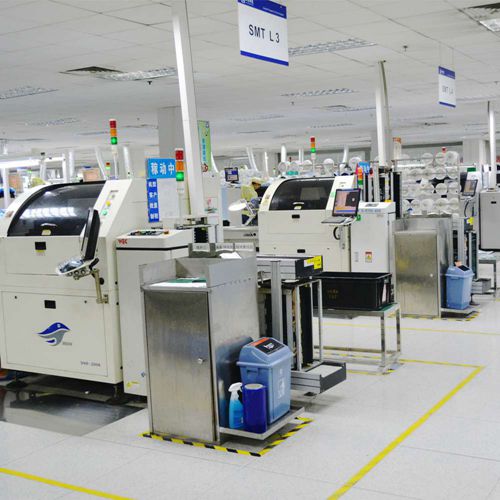
SMT Production Line
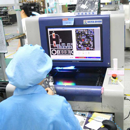
VCTAB486 AOI Equipment
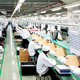
Production Assembly line
Soldering Production Line
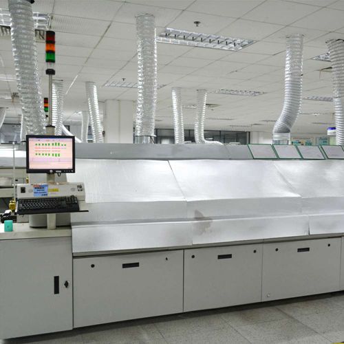
Reflow Soldering: XPM²820
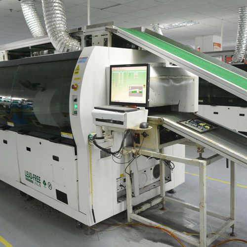
Automatic Wave Soldering WS-4501
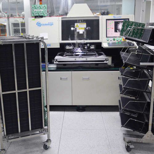
Automatic Insertion Machine
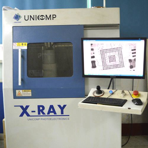
X-ray UNI-AX8200
PCB Assembly&Inspection Equipment List
| ITEM | Device Name | Model | Manufacturer | Qty | Remarks |
| 1 | Full Automatic Screen Printer | DSP-1008 | DESEN | 8 | |
| 2 | SMT Machine | YG200 | YAMAHA | 5 | 8 SMT Line |
| 3 | SMT Machine | YV100XG | YAMAHA | 3 | |
| 4 | SMT Machine | YG100XGP | YAMAHA | 19 | |
| 5 | SMT Machine | YV88 | YAMAHA | 5 | |
| 6 | Reflow Soldering | 8820SM | NOUSSTAR | 4 | |
| 7 | Reflow Soldering | XPM820 | Vitronics Soltec | 3 | |
| 8 | Reflow Soldering | NS-800 II | JT | 1 | |
| 9 | Solder Paste Inspection | REAL-Z5000 | REAL | 1 | |
| 10 | Automatic Optical Inspection System | B486 | VCTA | 3 | |
| 11 | Automatic Optical Inspection System | HV-736 | HEXI | 5 | |
| 12 | X-Ray | AX8200 | UNICOMP | 1 | |
| 13 | BGA Re-work | MS8000-S | MSC | 1 | |
| 14 | Universal 4*48-pindrive concurrent multiprogramming system | Beehive204 | ELNEC | 3 | |
| 15 | Automatic Plug-In machines | XG-3000 | SCIENCGO | 2 | |
| 16 | Automatic wave soldering system | WS-450 | JT | 1 | 3 DIP LINE |
| 17 | Automatic wave soldering system | MS-450 | JT | 2 |
![]()
Certificates
We have gained the certificates like ISO9001:2015, ISO14001, RoHS, and UL.